The air inside a semiconductor fabrication plant does not move like the air in your living room. It is scrubbed, pressurized, and pushed downward through grated floors in a constant, laminar sigh. Humans inside these rooms do not wear clothes; they wear armor against themselves—interlocking layers of Gore-Tex and latex designed to trap the flakes of dead skin and stray eyelashes that constitute weapons of mass destruction at the three-nanometer scale.
For years, the geopolitical map of the world has been drawn by these ultra-clean rooms. If you wanted the fastest artificial intelligence, the sharpest military radar, or the most efficient smartphone, your designs had to travel through a very narrow bottleneck. Specifically, they had to pass through the lithography machines of ASML in the Netherlands, and then onto the silicon wafers handled by TSMC in Taiwan or Samsung in South Korea. If you liked this piece, you might want to read: this related article.
Then came the sanctions.
When the United States cut off Huawei’s access to these advanced Western tools, the conventional wisdom in Silicon Valley was clear: the Chinese tech giant had been put on ice. Without Extreme Ultraviolet (EUV) lithography machines—monolithic systems that use lasers to bounce plasma off mirrors to etch lines thinner than a strand of DNA—you simply cannot keep pace with Moore’s Law. You hit a wall. For another angle on this development, refer to the recent update from Gizmodo.
But walls look different depending on which side of them you are standing.
Consider a hypothetical engineer named Zhao. He does not work in a pristine, multi-billion-dollar facility in Hsinchu. He works in a windowless research lab in Shenzhen, staring at a computer screen under the buzzing hum of a fluorescent light that has been flickering since Tuesday. Zhao knows he cannot buy the Dutch machines. He knows the standard physics of chipmaking have turned into a legal barricade. So, he and his team stop trying to walk through the locked front door.
They start looking for the floorboards.
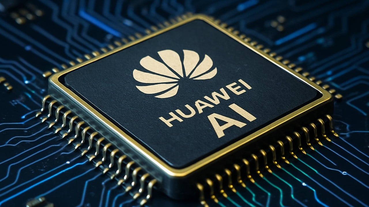
What Huawei recently unveiled isn't just a piece of hardware; it is a fundamental rewrite of how the industry measures progress. It is a new scaling law. For decades, the industry grew by shrinking the transistor. Huawei’s new approach acknowledges a harsh reality: if we cannot make the lines any smaller, we must make the architecture smarter. They have developed a methodology that clusters older, more readily available nodes in a massive, hyper-efficient matrix, using advanced packaging and custom software to make three separate pieces of silicon behave exactly like one seamless, ultra-thin chip.
The math behind it is deceptively simple but agonizingly difficult to execute.
If you cannot etch a five-nanometer line, you take two seven-nanometer lines and engineer an entirely new interconnect topology. You write algorithms that predict where data will bottleneck before the electron even leaves the gate. You use Deep Learning to optimize the physical layout of the chip, letting the AI design its own birthplace.
The results have sent a quiet shockwave through the industry. The performance gap between Huawei’s homegrown silicon and the cutting-edge chips rolling off TSMC’s assembly lines is no longer a chasm. It is a ditch. And Huawei is jumping it.
This is not just about corporate rivalry. This is about the illusion of technological monopolies.
When you deprive a highly funded, deeply motivated entity of a specific tool, you do not stop them from building. You merely force them to invent a different toolkit. Western analysts watched the shipping manifests, looking for signs of smuggled machinery, while Huawei was rewriting the textbook on silicon optimization. They shifted the battleground from raw material physics to systemic architecture.
Think of it as the difference between a sports car and a well-choreographed logistics fleet. Samsung and TSMC are building faster, lighter engines. Huawei, locked out of the titanium market, is building a network of interconnected vehicles that arrive at the destination at the exact same millisecond. To the user holding the device, the speed feels identical.
The implications stretch far beyond smartphone benchmarks.
We are entering an era of fragmented technology. For thirty years, the world operated on a unified hardware trajectory. Everyone used the same architecture, the same instruction sets, and the same manufacturing pipelines. That consensus is dead. By proving that a new scaling law can yield competitive AI and computing power without Western lithography, Huawei has created a parallel evolutionary track for technology.
There is a distinct vulnerability in realizing that the high ground you spent billions to fortify might not be the ground your opponent intends to take.
The standard industry reports will tell you about transistor density, yield rates, and thermal design power. They will present charts with neat, ascending lines. But those charts miss the sweat in the room. They miss the sheer, stubborn human willpower required to look at an export ban and see a design brief.
The gap is narrowing not because the machines got better, but because the thinking changed.
Somewhere in Shenzhen, the flickering fluorescent light has finally been replaced. The room is quiet, save for the rhythmic hum of a server rack testing the next iteration of a chip that wasn't supposed to exist. On the screen, a line of code finishes executing. The benchmark holds steady. The invisible barrier that was supposed to last a decade has just dissolved into a series of clever algorithms and rewired silicon.
The race hasn't stopped; the track has just split in two.