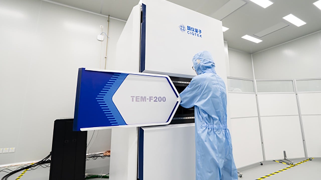
China’s push to deploy a domestic 0.1-nanometre transmission electron microscope is not a simple triumph of lab engineering over foreign monopolies. It is an urgent survival play to bypass export chokepoints, cut months-long maintenance delays, and give domestic chip and materials labs eyes that do not depend on Washington or Tokyo. Yet reaching 0.1 nanometres on paper is only the opening act. In real-world materials science and semiconductor failure analysis, hitting one tenth of a billionth of a metre is a baseline threshold, not a knockout blow against established leaders in Japan, the United States, and Europe.
Spend thirty years tracking precision hardware and you learn to read press releases with a magnifying glass. When a manufacturer announces a 0.1-nanometre electron microscope, the headline sounds like a frontier shattered. In reality, 0.1 nanometres equals one angstrom, right around the scale of atomic spacing in crystalline solids. Western and Japanese instruments have pushed past that mark for years using aberration correctors and sub-angstrom optics. The real story is not that a Chinese instrument can resolve down to 0.1 nanometres. The real story is why building that column inside China suddenly matters so much to global supply chains. You might also find this connected story insightful: Why a 2.5x Reception Boost Misses the Real Point of Laser Antennas.
Why Precision Optics Became a Geopolitical Flashpoint
For decades, high-end electron microscopy looked like one of the quietest oligopolies in science. If a university or a chip fab needed an advanced transmission electron microscope—often abbreviated as TEM—the shortlist was familiar. Japanese makers like JEOL and Hitachi High-Tech, alongside American-rooted Thermo Fisher Scientific, built the instruments that anchored materials research and semiconductor diagnostics. Buyers paid steep prices, waited on custom builds, and relied on specialized service engineers who knew every quirk of the vacuum column and high-voltage supply.
That quiet market turned noisy as export controls tightened around advanced computing, chipmaking tools, and dual-use research hardware. Even when an instrument is not banned outright on day one, compliance friction slows everything down. Export licenses take time. Spare parts get scrutinized. Field engineers face travel, vetting, or policy hurdles when servicing equipment inside restricted labs. As extensively documented in latest articles by Gizmodo, the implications are notable.
Imagine a hypothetical materials lab in Hefei or Shenzhen running defect analysis on a new gate-all-around transistor structure. If a high-voltage component or vacuum valve fails on an imported column and service takes eight weeks, the research schedule breaks. That is not an abstract trade debate. That is lost months on a wafer or battery cathode development cycle.
Domestic makers like CIQTEK and research institutes across China have moved aggressively to close that vulnerability. By focusing on a 200 kV field emission transmission electron microscope capable of 0.1 nm resolution, Chinese suppliers are targeting the exact workhorse band where industrial labs live. Not every lab needs an exotic ultra-high-voltage monster in a custom-shielded basement. Many need a dependable sub-nanometre column that arrives faster, costs less to maintain, and cannot be frozen by a foreign licensing office.
What 0.1 Nanometres Actually Means Under the Hood
To judge whether a 0.1-nanometre column threatens established rivals, you have to look past the marketing number and examine how electrons behave inside the machine. Light microscopes hit a diffraction limit around hundreds of nanometres because visible wavelengths are simply too long. Electrons accelerated through tens or hundreds of kilovolts have wavelengths measured in picometres—trillionths of a metre—which is why electron beams can probe atomic structures.
Shorter wavelength alone does not guarantee crisp atomic imaging. Real resolution depends on keeping every source of blur under control.
- Electron source brightness and energy spread: A field emission gun concentrates electrons into a tight, coherent beam, while tighter energy spread reduces chromatic blur when electrons pass through a specimen.
- Lens aberrations: Magnetic lenses bend electron beams, but they do so imperfectly. Spherical aberration smears point sources into disks unless corrected by multi-pole electromagnetic optics or carefully tuned imaging conditions.
- Mechanical and thermal stability: At 0.1 nanometres, air currents, floor vibration, acoustic hum from nearby chillers, and tiny shifts in power-supply current can smear an atomic column into a streak.
- Sample preparation and radiation damage: Thinning a semiconductor cross-section or battery electrode without introducing artifacts—and imaging light elements before the beam knocks atoms out of place—often limits practical results more than the microscope itself.
A hypothetical example makes the distinction clear. Suppose two microscopes both advertise 0.1-nanometre resolution under ideal test conditions. One holds that sharpness only on a sturdy crystalline standard during a quiet night shift, while its detector reads out slowly and its column drifts under heavy mapping workloads. The other maintains sharp contrast during rapid elemental mapping, automated tilt series, and multi-hour sample runs. On a spec sheet, they look equal. On a factory or research floor, they belong to different tiers.
Where China Gaining Ground Hurts Most
If analysts look for a dramatic overnight collapse in Western or Japanese market share, they are looking in the wrong place. Top-tier atomic-resolution microscopy still depends on deep ecosystem advantages: ultra-stable high-voltage power supplies, precision-machined magnetic pole pieces, low-noise direct electron detectors, mature alignment software, and decades of application recipes across thousands of customer sites.
Instead, the real shift happens in three quieter areas that compound over time.
| Dimension | Legacy Foreign Leaders | Emerging Domestic Chinese TEMs | Practical Impact |
|---|---|---|---|
| Supply & Service Continuity | Subject to export rules, licensing checks, and cross-border logistics | Built and serviced domestically without foreign export choke points | Lower risk of prolonged downtime for domestic labs |
| Core Optical & Detector Maturity | Decades of sub-angstrom, cryo, and analytical refinements | Rapid catch-up at the 0.1 nm workhorse tier | Foreign tools still lead at extreme analytical frontiers |
| Total Cost & Adoption Speed | High capital and service costs; longer lead times | Competitive pricing and faster local support inside China | Accelerates domestic training, iteration, and volume scale |
First is import substitution inside China. Every domestic university, battery maker, catalyst lab, and chip research group that buys a homegrown 0.1-nanometre TEM reduces foreign vendor leverage in one of the world’s largest science and manufacturing markets. Even if foreign firms keep the hardest research contracts, losing the middle and upper-middle volume tier erodes scale and aftermarket revenue.
Second is engineering feedback loops. A microscope improves because engineers watch thousands of real samples fail, drift, overheat, or behave unexpectedly in the field. When domestic instruments go into active daily service across Chinese labs, local teams collect that operational data directly instead of learning second-hand.
Third is the broader leverage game. Export controls do not operate in a vacuum. When one side restricts advanced tools or components, the other looks for chokepoints of its own—from specialty chemicals and critical minerals to rare earth elements and magnet materials used across precision actuators and industrial gear. A domestic electron microscope weakens one lever of external pressure on China’s materials and semiconductor ecosystem.
The Blind Spots in the Hype
Any serious assessment has to push back against two opposite myths. One myth says Chinese hardware cannot compete at the frontier because foreign firms had a head start. History shows latecomers in precision manufacturing—from cameras and machine tools to solar cells and electric vehicles—rarely stay stuck at the bottom once state backing, domestic demand, and engineering talent align.
The opposite myth is just as lazy: that announcing a 0.1-nanometre microscope means China has already matched the best analytical electron microscopes on earth. Resolving a lattice spacing is not the same thing as running high-throughput, automated atomic-scale spectroscopy on fragile materials day after day. Software workflows, detector sensitivity, long-term drift stability, and global customer trust take years of grinding iteration to earn.
There is also a subtle trap in how commentators frame this race. A microscope does not manufacture a 2-nanometre chip by itself. It is a diagnostic instrument—a magnifying glass for inspecting structures, defects, interfaces, and crystal grain boundaries. Having a domestic 0.1-nanometre TEM helps researchers spot what went wrong inside a material or device stack, which speeds up troubleshooting. It does not magically replace lithography scanners, deposition tools, or etch systems.
What US, Japanese, and European suppliers cannot afford to do is treat 0.1-nanometre domestic instruments as mere copies or low-end curiosities. History punishes incumbents who mistake a narrower performance gap for a permanent moat.
Watch who wins the service and software layer over the next five years, not who wins the first resolution headline.